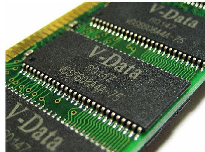
Synchronous DRAM or SDRAM is the current standard for DRAM.
That isnt to say that it runs at the same clock speed as the CPU.
But it has an internal clock, and the CPU knows it.
Part of the problem is that when writing data to DRAM.
The data must be provided simultaneously as the command to write the data.
With asynchronous DRAM, this happened by simply allowing more than enough time for the operation to complete.
This practice, however, left the I/O bus idle.
Synchronous DRAM uses an internal clock to synchronize the transfer of data and the execution of commands.
This lets the memory controller time operations make optimum use of the I/O bus and ensures higher performance levels.
Each bank essentially operates independently internally.
Within a bank, only one row can be open at once.
This design prevents the I/O bus from sitting idle.
At the same time, a new read or write operation is being queued up, increasing efficiency.
One way to think about this is by adding a third dimension to a two-dimensional array.
you’re able to still only read or write data from one place at a time.
But you might prepare another row in a different bank while one is being interacted with.
Another benefit of SDRAM comes from the inclusion of timing data on a chip on the memory.
It can also be possible to manually override these controls, allowing the RAM to be overclocked.
Overclocking RAM also comes at the risk of instability but can offer advantages in some workloads.
Improvements Over Time
The actual memory clock speed hasnt increased much since the release of SDRAM.
The first iteration of SDRAM received the retronym SDR.
This is short for Single Data Rate to distinguish it from the later DDR or Double Data Rate memory.
These types, as well as many other forms of DRAM, are all examples of SDRAM.
The clock cycle of the DRAM chip controls the time between the fastest operations of DRAM.
For example, reading a column from an open row takes a single clock cycle.
Both can be controlled independently and have been upgraded over time.
The internal clock is the speed of the memory itself and directly influences the latency.
This clock speed, combined with the width of the I/O bus, influences the bandwidth.
Both clocks are linked and are critical to the high performance of SDRAM.
DDR3 still offered 100MHz memory clocks, though it also standardized clock speeds up to 266.6MHz.
The DDR5 standard also starts with a memory clock of 200MHz.
Conclusion
Synchronous DRAM is the primary pop in of DRAM in use today.
It is the basis for system RAM and VRAM in graphics applications.
The clocks that control SDRAM are critical to its high performance.
By having these timings known, they can be optimized for peak performance.
